


Automated Optical Inspection (AOI 500)

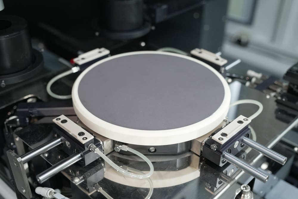
Advanced Optical Inspection System for Semiconductor Wafers


  • Ultra-Fine Defect Detection (as small as 0.5μm)
  • Non-Periodic Scan Technology (HyVISION Only)
  • Real-Time Processing Architecture
    (Distributed/Multi-Processing, Multi-Threading)
  • High-Resolution Telecentric Illumination
  • High-Performance LED Lighting 

  • AI Deep Learing Algorithms
    (Wafer Teaching/Defect Detection/Defect Classification)

Key Features Technical

Built on our core capabilities and differentiated technologies,
we present the key features and technical strengths that deliver new value to our customers.

Automated Optical Inspection
Automated Optical Inspection Inspection Site Review Site

* Click a marker to explore each zone.

Main Features


1

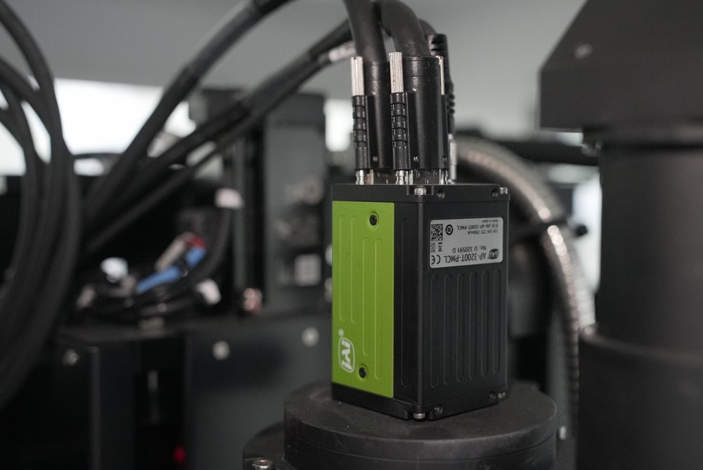
Ultra-Fine Defect Detection

Provides high-resolution inspection technology that

precisely detects ultra-fine defects and external 

foreign matter at the 0.5um level.

2

Non-Periodic Scan Technology (HyVISION Only)

Supports both periodic and non-periodic scan methods 

to flexibly respond to various inspection conditions, 

enabling inspection of fixed patterns as well as irregular 

environments.

3

Automated Wafer Vision Teaching

Automates Wafer / Vision Teaching to reduce 

operator dependency and shorten setup time.

4

Real-Time Processing Architecture

Real-time inspection system based on distributed 

/ multi-processing / multi-thread architecture.

5

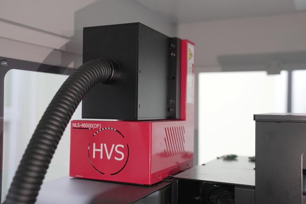
High-Resolution Telecentric Illumination

Applies telecentric illumination to secure uniform 

light distribution and distortion-free high-resolution 

images, providing a precise inspection environment.

6

High-Performance LED Lighting

Applies LEDs with +/-2% brightness deviation and up to 

20,000 hours lifetime to improve image quality consistency 

and maintenance efficiency, implementing an optimized 

inspection environment through in-house light source technology.

7

AI-Based Defect Detection & Classification

Combines rule-based algorithms with AI deep

learning to improve inspection accuracy and scalability.

Application

CONTACT